Wafer mapping high-speed scanning of transparent wafers
Wafer mapping high-speed scanning of transparent wafers
Transparent layers can make it difficult to capture consistently sharp images during photonic wafer inspection. Nobleo’s wafer mapping feature helps maintain precise autofocus across the wafer surface, supporting reliable, high-speed scanning at high magnification.
Autofocus challenges with transparent photonic wafers
Photonic wafers typically have a transparent top layer to enable light to be coupled in and out of these wafers. This transparent layer makes it difficult to autofocus, which leads to blurry images. The requirement for an accurate autofocus sensor is more and more critical as the magnification of the imaging system increases.
Nobleo has been developing a wafer mapping feature to measure the wafer surface topology to prevent blurry images while scanning. The wafer mapping feature uses input of an autofocus sensor provided by PI (static sensing resolution of less than 3 nm), which is well below the DOF of the scanning system.
Measuring wafer surface topology with high precision
The sensor readings of the PI sensor are used to measure the surface topology of a test wafer without a transparent top layer. The surface profile shows a smooth surface profile with autofocus distances between 158 to 166 µm.
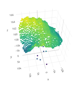
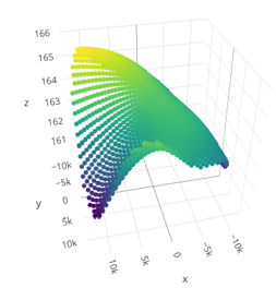
Figure 1: The measured height profile (left) and the fitted curve through the set of points to parametrize the surface topology
High-speed wafer scanning with accurate autofocus setpoints
A surface profile has been fitted to generate an autofocus setpoint for specific (X,Y) positions on the wafer. The fit error between the model and the measured profile is less than 1 µm (3σ).
By executing a wafer mapping scan sequence prior to scanning the wafer, it is possible to generate autofocus setpoints to accommodate for (local) height variations on the wafer. The autofocus sensor allows for scanning rates of up to 30 kHz. Executing such a wafer mapping scan sequence can be done efficiently, restricted primarily by the speed of the motion system of the scanner.
For high magnification microscopy the height variations on the wafer can be significantly larger than the DOF of the sensor. The images below were taken with an image resolution of 125 nm per pixel and a depth of field of ± 1 µm. As a result, not all details in an image can be imaged sharply (see Figure 2). When the wafer mapping is used to generate autofocus setpoints, all images on the wafer are consistently in focus.
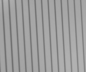
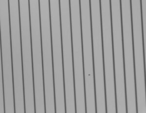
Figure 2: An image taken of a set of waveguides with the default autofocus settings suffering from focus issues caused by a transparent top layer (left) and the same area where the autofocus distance has been set using the wafer mapping output (right).
Wafer mapping for transparent layers and copper tracks
The wafer mapping feature can also used to generate autofocus setpoints for specific layers on the wafer. This can be the case for wafer with transparent top layers and or copper tracks which introduce a typical height increase of > 20 µm. An example of this application is shown below.
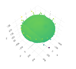
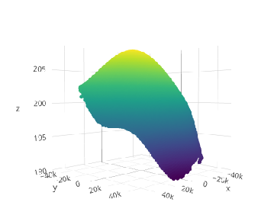
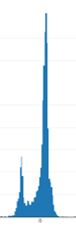
Figure 3: The surface profile measured with the autofocus sensor (left) is used to fit a parametrized surface shape (middle); the difference between the fitted curve clearly shows 2 peaks that are linked to the top surface of the wafer and the (visible) layer that seem to match with the thickness of the transparent top layer of the wafer.
The example illustrates that the wafer mapping feature can be used to make scans of specific layers: for example copper tracks with a height of 20 µm relative to the wafer substrate.
Wafer pocket measurements for precision bonding
A third use case that is explored is to use the autofocus sensor to accurately measure the surface topology of specific details on a wafer (such as pockets).
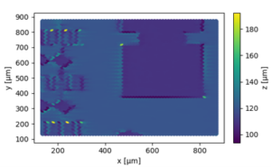
Figure 4; Measuring the depth of a pocket on a wafer with an autofocus sensor.
Photonic chips often require hybrid or heterogeneous integration to create a functional unit. This often requires accurate positioning of a component on another component. The wafer mapping sequence can also be used to measure the orientation of a pocket on a wafer relative to the substrate as an input for wafer bonding, die to wafer bonding, wafer-to-wafer bonding, etc.
Every micron matters. Don’t let focus issues compromise your wafer inspection. Facing challenges with transparent wafers? Share your application with our experienced engineers through the contact form and discover how wafer mapping could make a difference.