Improving Wafer Defect Detection with Design-Based Masking
Masking irrelevant areas on a wafer to improve defect detection performance
Improving wafer defect detection requires focusing on what truly matters. By combining design-based masking with machine learning, Nobleo enables more accurate defect detection on photonic wafers while reducing irrelevant information and improving network sensitivity.
Wafer defect detection: focusing on critical structures
The assessment of a photonic wafer by humans is typically done by focusing on critical design elements. A quality engineer will look at particles in areas that will cause performance issues on the wafer. For example, particles on waveguides or on grating couplers.
Design-based masking using GDS files
Nobleo has taken this idea and developed a masking feature that uses design information to focus on relevant areas only: an alignment marker design file (GDS). The Nobleo software can find these markers on the microscope images and calculates a mapping between pixels and wafer coordinates. A design file (GDS) of the to-be-inspected components. The Nobleo software automatically masks pixels which are not part of a component.


Figure 1: The original image with a set of waveguides (left) is processed such that all areas that are irrelevant are masked (middle); the machine learning networks evaluating the wafer surface will only consider the waveguide structures (right).
Benefits of masking for machine learning defect detection
Applying the masking feature to a scan image for defect analysis has multiple benefits.
- Better network performance
This approach allows the network to only focus on relevant details in an image. This boosts defect detection performance.
- Less clutter
The network performance is not degraded by serial numbers, alignment markers and/or metrology features on the wafer. A process engineer doing an assessment of the wafer only needs to assess defects on critical wafer locations.
- Analyze details accurately
The masking feature can be used to train a machine learning network to assess very specific repetitive shapes on the wafer using position information from the wafer design (for example: grating couplers). By zooming in on a specific detail, the machine learning network assessing the quality can be lightweight and fast.
Testing the masking feature on electrical test structures
The alignment accuracy (absolute accuracy of the wafer stage) and image distortions are a limiting factor as to how accurately the mask fits to the structures under test.
The feature was tested on a set of electrical test structures.


Figure 2: A photonic wafer with electrical test structures (top) is analyzed with an anomaly detector to check for process errors that impact the impedance of the interconnects. A part of the test structures (left) is analyzed with an anomaly detector (right).
Improving anomaly detection sensitivity with masked images
The output of the anomaly detector shows that the anomaly detector triggers on process variations (marked with red rectangles). The sensitivity of the detection can be significantly improved by using the masking feature. Instead of feeding the network the entire image, only the areas close to a waveguide have to be considered by the network.
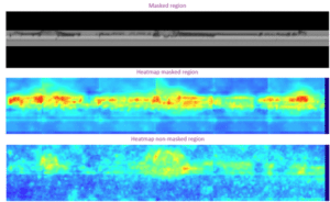

Figure 3: A damaged electrical interconnect (top) is inspected with a network trained on masked images (middle) and a network trained on the original image (bottom). The heatmaps clearly show that the masking feature “helps” the anomaly detector to focus on the process errors at the edges of the interconnect. The network trained on the original image is significantly less sensitive. The network sensitivity is improved drastically by using the masking feature.
More accurate defect detection and future applications
General defect detection focuses on the complete images even if these image areas are irrelevant. The defect defection (from masked images) only highlights relevant image areas, thereby dramatically improving the sensitivity of the network.
Applying the masking feature makes a huge difference in algorithm performance. It might even be possible to associate anomaly scores of the network with impedance measurements to predict electrical properties of interconnects based on machine learning assessments.
Want to learn more about improving wafer defect detection with design-based masking? Fill in our contact form for more information.