The changing demands of semiconductor manufacturing
Three experts on the future of semiconductor manufacturing
For decades, the chip industry was driven by one clear principle: fitting more transistors onto the same piece of silicon. Moore’s Law captured that ambition and helped deliver extraordinary gains in computing power while reducing the cost per transistor. However, continuing to improve performance by shrinking transistors alone is becoming more complex and expensive, while applications such as AI demand ever more computing power and faster data transfer. The industry is therefore exploring new ways to improve performance, with major implications for chip design, advanced packaging and the equipment used to manufacture semiconductors.
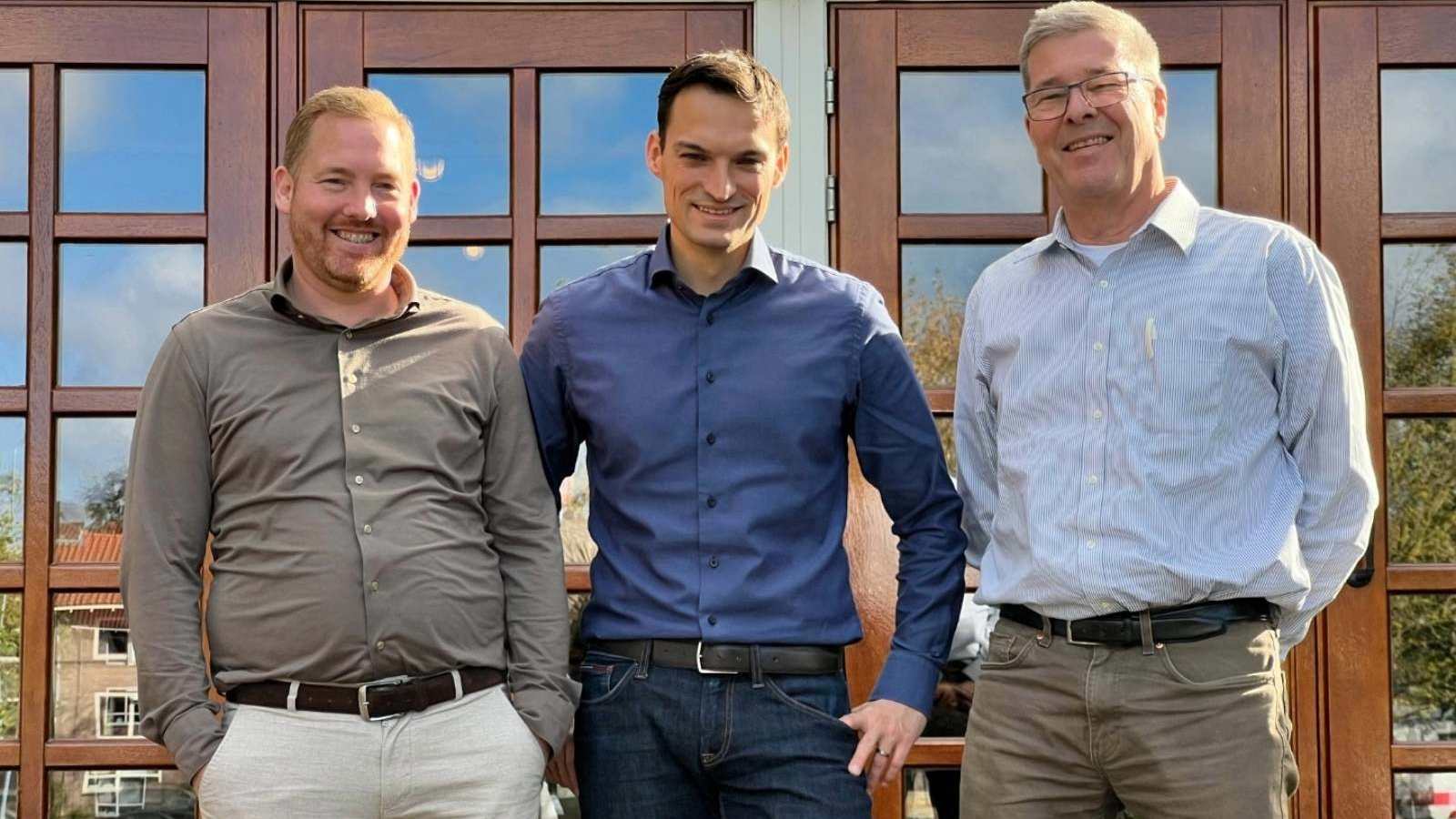
Nobleo colleagues Ruud van der Aalst (Business Unit Director Mechatronic Systems), Niels Koenraad (System Architect) and Frank Sperling (CTO and co-founder) share their views on where the industry is heading and the engineering challenges this creates.
Beyond Moore’s Law: the future of semiconductor manufacturing
In 1965, Gordon Moore observed that the number of transistors that could be fitted on a microchip was increasing rapidly. A decade later, he predicted that that number would double every two years. Moore’s Law has driven decades of semiconductor innovation, making increasingly powerful computing available at ever lower costs. But keeping that pace through transistor shrinking alone is becoming increasingly difficult. “For a long time, the industry could step up computing power by simply making the transistor smaller,” Ruud says.
“But keeping Moore’s Law going is getting steadily harder, both physically and economically. We have come to a point where we have to look at other ways to increase computing power, shifting from scaling the individual chip to scaling the complete system.”
One way to do this is by moving away from putting every function on a single, large chip. Instead, manufacturers divide a design into specialised chiplets, each performing a particular function, e.g. GPU, memory, or I/O, and integrate those functions into one package. Different chiplets can be manufactured using different process technologies and then integrated into one single system through advanced semiconductor packaging.
Advanced semiconductor packaging for AI
The growing demands of AI are accelerating this shift towards system-level integration. Modern AI processors can handle enormous amounts of computation, but processing data is only part of the challenge. As computing performance increases, moving data between memory and the compute cores can become a bottleneck often referred to as the memory wall.
“The bottleneck is getting the data to the processor fast enough,” explains Niels. “2.5D packaging, i.e. placing multiple dies side by side on a silicon interposer, or 3D packaging by vertically stacking dies, can help by bringing the High Bandwidth Memory closer to the compute core. The more components you integrate however, the more difficult the manufacturing process becomes. Stacking more memory layers, for example, creates shorter connections and higher bandwidth, but every additional layer has to be aligned and connected extremely accurately. A small error in one layer can affect the entire stack.”
As data transfer demands continue to rise, the semiconductor industry is also exploring co-packaging solutions that bring photonics closer to the compute and memory elements. By integrating photonics into chiplet-based packages, data can be transferred optically over short distances, helping support higher bandwidth while reducing the energy required to move data. As a result, the benefits of advanced packaging technology depend on the ability to assemble increasingly complex structures with a high degree of precision and reliability. This places greater demands on the equipment used to manufacture and assemble these packages.

From left to right: Niels Koenraad, Ruud van der Aalst, and Frank Sperling share their perspectives on the future of semiconductor manufacturing.
Precision engineering in semiconductor equipment
As semiconductor equipment becomes more complex, achieving the required precision takes more than highly accurate mechanical components. Machines have to move quickly while maintaining extremely tight tolerances. At the same time, larger optical systems, moving masses, and even cooling systems can introduce vibrations that affect measurement and motion accuracy.
“The more accurate you get, the more problems appear that you never had to consider before.”
“Suddenly dynamics, thermal behaviour and cleanliness become critical.” says Niels. “You can have a machine that looks perfect on paper, but once you start moving it or switch on the water cooling for example, you discover vibrations that affect the accuracy.”
For Frank, this illustrates why semiconductor equipment needs to be approached through system engineering rather than as a collection of individual components. “Many of the difficult engineering questions arise where disciplines meet,” he says. “A mechanical design can be perfectly sound on its own, but that does not tell you how the complete machine will behave. Actuators, mechanical, control loops, thermal effects and measurement all interact. You have to understand where the disturbances come from, model them, change the design or control strategy, and then measure whether your solution actually works. That cycle of analysis, design, measurement, and iteration is where a lot of the real engineering happens.”
Bridging front-end and back-end semiconductor manufacturing
The need to consider the complete system also matters across different stages of semiconductor manufacturing. Traditionally, front-end processes demanded nanometre precision, while back-end manufacturing placed greater emphasis on design for cost /design for value and total cost of ownership. Advanced packaging technology is bringing the two closer together: back-end processes increasingly require extreme accuracy, while front-end equipment must also meet growing demands for cost-effectiveness and manufacturability.
Frank explains how Nobleo’s experience across both areas helps address these changing requirements.
“We understand the demands of front-end equipment, where even the smallest deviation can matter, as well as the cost and production pressures in the back end. Having worked in both worlds means we can bring ideas and experience from one into the other.”
What works in one area can often help solve a challenge in the other, provided you understand the specific requirements of the application.
Designing semiconductor equipment for industrialisation
Meeting the technical requirements is only one part of developing semiconductor equipment. In the semiconductor industry, time-to-market is critical: if a machine is not ready when the market needs it, a company can miss its market window. Delays in development or unexpected manufacturing challenges can mean losing valuable time and the opportunity to bring a new technology to market when it matters most.
That is why Nobleo considers industrialisation from the start of the development process. Through its Design House+ approach, the team looks beyond technical performance to include manufacturability, cost, and production requirements from the outset. Considering these factors early helps identify potential obstacles before they become costly problems and ensures that design decisions support both the machine’s performance and a realistic route to production.
“A solution has to do more than meet its technical specifications,” says Ruud. “It also needs to be realistic to manufacture at the required quality, cost, and volume. If manufacturability and production requirements are only considered at the end of development, you may discover that a technically good design is difficult or expensive to produce. By considering industrialisation from the beginning, you can make better decisions earlier on in the process and avoid unnecessary and costly redesign.”
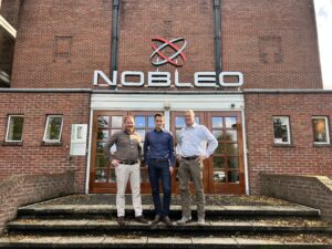
From left to right: Ruud van der Aalst, Niels Koenraad, and Frank Sperling in front of our office in Eindhoven.
Working alongside customers
Addressing these challenges requires close collaboration between the equipment manufacturer and the specialists involved in the development. Nobleo’s engineers work as an extension of the customer’s development team, bringing together the disciplines needed for a specific challenge. The customer retains ownership of its product, process, and intellectual property, while Nobleo contributes the engineering expertise needed to move the development forward.
“We don’t come in with the idea that we know the customer’s process better than they do, says Ruud. “They are the experts in their product and their application. We bring our experience in mechatronics, precision engineering and dynamics & control and liaise with the customer to combine all that knowledge.”
Making the next step possible
For semiconductor equipment manufacturers, the challenge is to keep pushing technological boundaries while managing the risks and uncertainties that come with innovation. Nobleo can help tackle these challenges, bringing the expertise and practical problem-solving needed to move from a difficult technical question to a workable solution. This gives original equipment manufacturers a partner to turn to when the next development step calls for a fresh perspective or specialist knowledge.
Discover how Nobleo’s advanced mechatronic development expertise can support your next engineering challenge.