

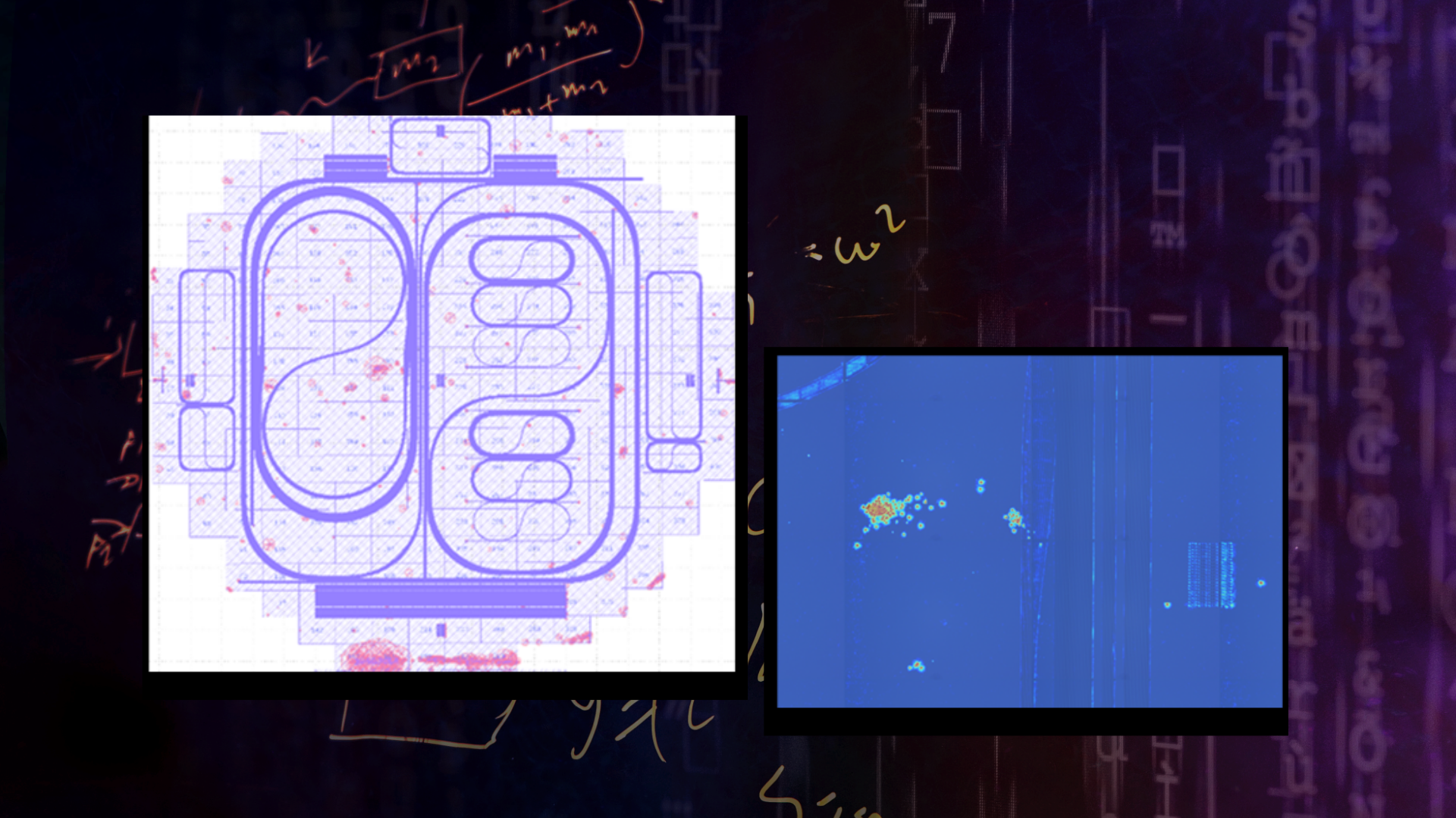
The Photonic Visual Inspection Tool (PVIT) is designed to set up quality inspection for high-mix, low-volume production, with the flexibility to scale and evolve alongside production growth throughout the manufacturing lifecycle. By reducing active testing time, it helps customers increase throughput and improve overall efficiency.
What PVIT delivers
Efficient visual inspection of photonic wafers - optimized for high-mix R&D and production ramp-up
The photonic industry demands ever-higher quality standards and production efficiency. Even the smallest defect can impact performance and yield, driving the need for reliable, automated inspection methods. The Photonic Visual Inspection Tool supports this challenge with intelligent, vision-based analysis that combines speed, precision and adaptability.
PVIT delivers fast and intelligent visual analysis for photonic wafer inspection. Within just five minutes, users can create detailed defect maps for new designs, gaining immediate insight into wafer quality. The system integrates seamlessly with standard laboratory microscopes already in use, eliminating the need for additional equipment.
Its advanced AI automatically detects defects while continuously learning the user’s specific quality standards. A dual visualisation system combines heat maps for an overall quality overview with detailed defect maps for in-depth precision analysis. PVITs smart prioritisation instantly highlights defects in critical wafer areas, enabling faster decision-making. In addition, cross-process tracking allows users to follow defect development across manufacturing steps, providing a complete view of quality progression and process impact.
How it works
Collaborative Implementation
PVIT is installed on-site with close collaboration to ensure perfect integration with your existing workflow. Together, we establish:
- Interface connections to your wafer scanning systems
- Design data integration (GDS files, areas of interest, alignment markers) to assess function-critical design elements
- Configure defect categories in-line with existing quality guidelines
Automated Intelligence Pipeline
- Data Ingestion: Automatically loads wafer scans and design information
- AI Training: Trains specialised anomaly detection networks for inspection tasks
- Analysis & Visualisation: Generates defect reports and anomaly heat maps
- Continuous Learning: Improves accuracy through annotation feedback and iterative training
Our capabilities with PVIT

Defect Types
Preconfigured to accommodate for customer specific defect categories to ensure that defect detection is in-line with existing quality standards.

Wafer Maps
Render defect maps in GDS format that can be overlaid on top of a design file to assess criticality of a detected defect.

Dashboarding
Output test reports and image data in a custom file format to enable our customers to create their own wafer quality dashboards.

Data Import
Includes a customised interface to use off-the-shelve microscopes to build custom defect inspection algorithms.

Data Backup
PVIT provides a backup feature to prevent loss of (annotated) data.

Data Security
PVIT is installed on-site. The scan images are stored locally (no cloud), without dependencies on 3rd party software or an internet connection.

Training of Staff
Nobleo supports customers for a 3-month period to ensure that wafer designers know how to efficiently operate the tool, and supports process engineers with the iterative improvement of the defect detection algorithms on distance.
Defect Types
Preconfigured to accommodate for customer specific defect categories to ensure that defect detection is in-line with existing quality standards.
Wafer Maps
Render defect maps in GDS format that can be overlaid on top of a design file to assess criticality of a detected defect.
Dashboarding
Output test reports and image data in a custom file format to enable our customers to create their own wafer quality dashboards.
Data Import
Includes a customised interface to use off-the-shelve microscopes to build custom defect inspection algorithms.
Data Backup
PVIT provides a backup feature to prevent loss of (annotated) data.
Data Security
PVIT is installed on-site. The scan images are stored locally (no cloud), without dependencies on 3rd party software or an internet connection.
Training of Staff
Nobleo supports customers for a 3-month period to ensure that wafer designers know how to efficiently operate the tool, and supports process engineers with the iterative improvement of the defect detection algorithms on distance.
Service Features and Benefits
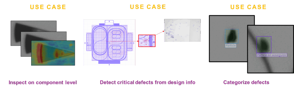
PVIT supports three core inspection workflows:
1. Component-level inspection: Automated analysis of individual components
2. Critical area monitoring: Targeted defect detection in critical wafer areas
3. Custom defect classification: Categorization aligned with customer-specific defect categories
Implementation Process
The system processes wafer scan data using machine learning algorithms to identify defects and quality issues. Wafer designers provide GDS files with AOI definitions that specify which areas to inspect. Nobleo works with quality teams to set up defect categories based on manufacturing requirements. Once set up, the system can convert scan data into defect maps and heat maps within 5 minutes. Any visual assessment of wafer scan images can be used to develop automated defect inspection algorithms in a consistent manner. The output is used for quality dashboards to monitor process variations and supports die binning to reduce active testing.
System Specification
Software Features
- Import wafer scan data from standard image formats
- Display large image files without noticeable time delays
- Automated conversion of wafer scans into image sets per component or die
- Web-based annotation interface to assign defect types to defects in images
- Tooling to train your own anomaly and object detection networks
- Render heat and defect maps to support visual assessment
- Load images that contain critical defects within a single click
Customization options
- Load wafer scan data from local network or directly from lab microscope
- Send test results to data management systems
Hardware specifications
- Processor: Intel® Core i9
- Memory: 64 GB RAM
- GPU: NVIDIA RTX™ A4500 20 GB GDDR6
- Storage: 8 TB storage
Services Available
- Technical Support
- Installation and Setup
- Maintenance
- Application Support
- Hardware Support
- Guaranteed Warranty
Coming Soon...
Automatic batch processing pipelines to run a range of trained networks on a specific wafer design.
For more information, use the contact form below.


Get in touch
"*" indicates required fields
Can I help you?