Inline wafer scanning
Inline wafer scanning
Reliable wafer inspection requires more than high-resolution imaging. Scan speed, image quality and accurate positioning all play an important role in photonic wafer manufacturing. Working alongside IMS, LioniX International and Settels Savenije, Nobleo has contributed to the development and validation of an inline wafer scanning solution that combines high-magnification optical inspection with a demonstrated throughput of 10 4-inch wafers per hour.
High-resolution inline wafer inspection
IMS is a supplier of high-precision manufacturing equipment based in Almelo in the Netherlands. IMS has been developing a Photonic Visual Inspection Tool for wafer level inspection called Helios. The machine is an inline metrology tool designed to perform high-magnification scanning of wafers at a rate of 10 wafers per hour (4-inch wafers).
The system can scan wafers with a bright field illumination and a dark field illumination to highlight surface irregularities on the wafer. The PVIT tool can scan wafers at a resolution of 500 nm per pixel and at 125 nm per pixel.

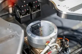
Figure 1 The Helios system developed by IMS designed to automate optical inspection of Photonic Integrated Chips (PIC’s).
Validation on the TriPleX® photonic platform
The scanning function was validated in close cooperation with Lionix International in Almelo. Lionix manufactured a set of test wafers covering the different surface materials used in the manufacturing of their TriPleX® wafer technology platform. The PVIT tool showed consistent image quality for the function critical processing steps.
Autofocus optimisation and scan performance
Nobleo developed a wafer mapping feature to ensure in-focus images while scanning wafers with transparent top layers. Nobleo tuned the control loop for the autofocus system together with experts from Settels Savenije. The objective of the tuning task is to maximize scan speed without compromising on image quality. Scanning of the 4-inch test wafers at a rate of 10 wafers per hour was demonstrated.
Microscope alignment and qualification
The development of tooling to install and qualify the microscopy system was done by Nobleo. The installation of the high-magnification microscope requires accurate alignment and qualification of the microscope in the machine. Nobleo also developed software tools to align the microscope relative to the chuck, to tune the focus of the microscope, to quantify the optical distortions and the homogeneity & consistency of the illumination.
Flexible wafer scanning with test recipes
The PVIT tool can execute test recipes defining where to scan. The machine can inspect critical components (such as grating couplers) at a set of (x,y) locations on the wafer or scan a set of AOIs on the wafer. The definition of where to scan is defined in a test recipe. The recipe editor has been developed by Workfloor.
The microscope unit of the PVIT tool is designed by Settels Savenije and can be optimized for specific use cases. The microscope can be modified to accommodate for custom applications (infrared illumination, higher levels of magnification, etc.). The tool is available for industry partners to scan wafers to understand the capabilities of the tool.
Custom AOI scanning solutions
Together with our consortium partners, we have the expertise to develop high-quality AOI scanning solutions for photonic wafers. We have also been in contact with companies looking to integrate an AOI scanning module into their wafer processing equipment.
Depending on the application, we can customise the existing microscope module together with Settels Savenije or integrate an alternative off-the-shelf solution from our partners in the semiconductor ecosystem. We are happy to explore which approach best suits your wafer testing or inspection requirements.
Extending wafer inspection with machine learning
Beyond high-resolution scanning, machine learning can help extract additional information from wafer images to support inspection and processing.
Nobleo can extend the scanning function with machine learning algorithms to help you:
- determine the wafer position to support wafer processing
- analyze process variations by analyzing (custom) metrology markers
- perform quality inspections of components on a wafer
- create a wafer defect map to assess wafer quality
- classify defects into custom defect types.
Discuss your wafer inspection challenge with us
Looking for a high-resolution wafer inspection solution or exploring the integration of automated optical inspection into your equipment? Our engineers would be happy to discuss the possibilities. Get in touch using the contact form below.