A generic approach to fiducial based wafer alignment
A generic approach to fiducial based wafer alignment
Accurate wafer alignment is essential for reliable inspection and processing in semiconductor and photonic applications. However, the wide variety of fiducial designs makes wafer localisation a challenge. Nobleo has developed a machine learning-based solution that can detect different fiducial designs without the need for a dedicated image processing algorithm for each marker.
The importance of accurate wafer alignment
A tool for testing and/or processing a (photonic) wafer almost always needs to understand the position of the wafer in the machine. The wafer localization function is function critical: if it fails the inspection tool will look in the wrong spot and/or wafer processing is done on the wrong location on the wafer. Needless to say, that this function should be both robust and accurate.
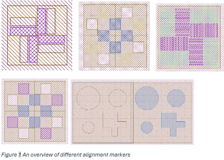
The default method to determine the position of a wafer is to locate fiducials on the wafer. It is up to the (photonic) wafer design and production facility to specify which fiducials are printed on the wafer. Designers and manufacturers all have their own preferences for specific and often custom fiducials.
A generic solution for fiducial detection
Traditionally, a custom image processing algorithm is developed for each individual marker. Nobleo has developed a machine learning based solution that works for arbitrary fiducial designs. The software solution is built around a transformer-based, detector-free, local feature matching network that finds correspondences between two images. This approach allows the same software solution to be applied to different wafer designs, reducing the need for marker-specific algorithm development.
The software solution requires the following inputs to work:
- A GDS descriptor defining the shape of the descriptor
- A list of X,Y positions in wafer coordinates with fiducial positions on the wafer.
Validation and performance
The implementation has been validated on a variety of different substrates and fiducial designs. The repeatability of the fiducial detection algorithm is well below 1 pixel (± 3σ).

The experimental results shown in Figure 2 were obtained with a high-magnification scanning microscope with a resolution of 125 nm per pixel. If the wafer contains a multitude of fiducials (one fiducial per die on a wafer), the set of observations can be used to estimate the orientation of the wafer relative to the sensor plane of the camera (image to wafer transform).
Beyond wafer alignment: system calibration
The image to wafer transform links the in-image pixel locations (u, v) to a (known) position on the wafer (X,Y). As the number of fiducials on the wafer increases, the in-image positions of the fiducials can be used to estimate a multitude of system properties:
- geometrical properties of the wafer.
- position accuracy of the stage.
- optical properties of the microscope.
This means that fiducial detection can contribute not only to accurate wafer positioning but also to a better understanding of the machine’s overall performance. The fiducial detection algorithms is an elegant way to identify system properties and to perform inline machine calibration. All of this to squeeze out the best possible system performance to process and/or inspect your wafer or product.
Facing challenges with wafer alignment or fiducial detection? Our engineers would be happy to explore how we can help. Get in touch using the contact form below.