Meet us at SPIE’26 to discuss the engineering behind advanced lithography
SPIE'26
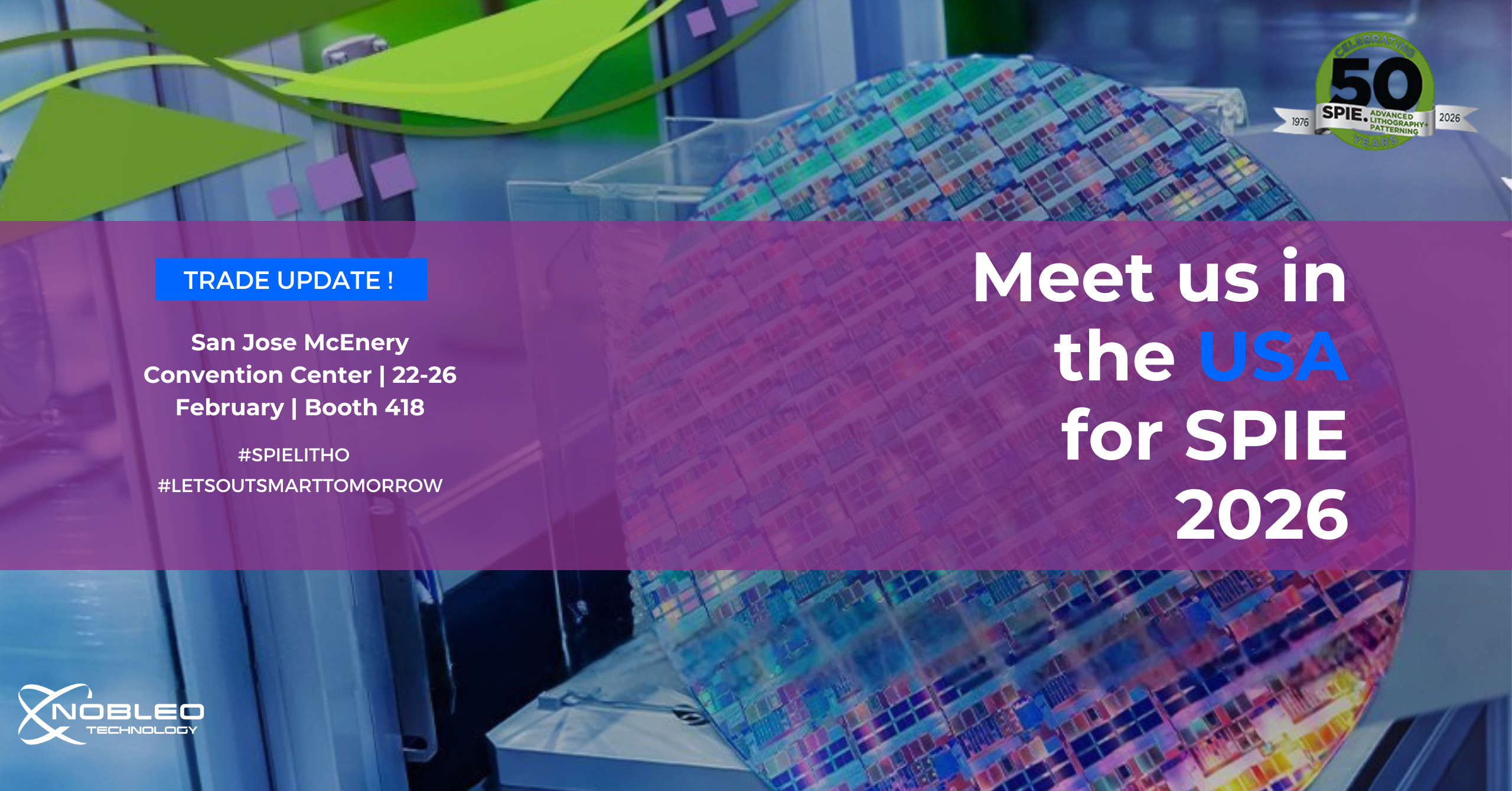
The SPIE Advanced Lithography and Patterning Conference in San Jose is where complex engineering challenges are discussed in depth. From 22–26 February 2026, we will be there to present our engineering capabilities in advanced lithography, mechatronics, and high-tech system development.
Advanced lithography places extreme demands on system accuracy, stability, and repeatability. We support customers in bringing complex, high-performance products to market by combining mechatronic system development, high-tech equipment, and dedicated test tooling with strong in-house design capabilities and a carefully managed supply chain. This multidisciplinary approach is carried by our Nobleans, who bring together expertise in advanced mechatronics, precision engineering, system dynamics, and servo control to address system-level challenges where mechanical design, control, and performance are tightly interconnected.
Long-term collaboration is central to how we work, with close cooperation with our customers to deliver lasting technical and operational value. We are available for technical and project-oriented conversations during the conference and beyond.
🤝 Meet us at Booth #418
📆 22–26 February 2026
📩 Contact Arie Leunis via arie.leunis@nobleo.nl for more information or to schedule a conversation during the conference.
spielitho AdvancedLithographyandPatterning letsoutsmarttomorrow mechatronics