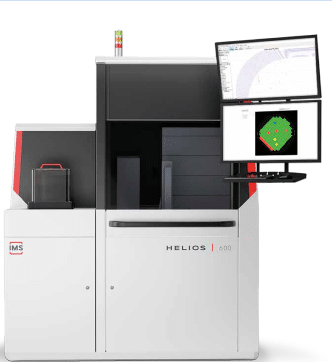
Scalable AI for photonic wafer inspection
Nobleo contributed core technologies, including high-speed camera control and AI-based defect detection, powered by our in-house NoblAI framework.
Scalable AI for photonic wafer inspection – Nobleo’s NoblAI in action
As photonic integrated circuits (PICs) continue to evolve, traditional inspection tools can’t keep up with the complex geometries and high-mix, low-volume production environments. To bridge this gap, we co-developed Helios: a tailored visual photonic wafer inspection tool.
Nobleo contributed core technologies, including high-speed camera control and AI-based defect detection, powered by our in-house NoblAI framework. This flexible platform helps manage datasets, streamline annotation and accelerate the deployment of tailored vision algorithms. In this project, NoblAI plays a central role in enabling efficient and accurate inspection across both early-stage development and industrial-scale production.
Helios inspects up to 10 wafers per hour at sub-micron resolution, enabling detection of defects as small as 100 nm and seamless overlay with GDSII design files.
📊 Defect maps are directly linked to design files (GDSII)
🌐 Experts collaborate remotely via web-based annotation
📈 The system supports a smooth transition from offline to inline inspection
This photonic wafer inspection solution is the result of a strong collaboration with IMS, Workfloor, Settels Savenije and LioniX International, under the MEKOPP and NXTGEN Hightech programmes.
Read here the full article about the innovation behind the photonic wafer inspection here: Mikroniek 2025-2 – AI PIC defect detection
Many thanks to DSPE and Mikroniek for the publication.
For more information about our image processing & machine learning expertise visit our dedicated webpage here:Image processing & Machine learning | Nobleo or feel free to contact us.