Photonic chip inspection tool
The photonic chip industry expects a rising demand and is investing in metrology equipment to improve yield.
Nobleo is developing a photonic chip inspection tool to perform a full-surface inspection of photonic integrated circuits (PIC). The inspection tool shall be able to perform a full-surface inspection of the photonic wafer to support process engineers to increase the maturity of their manufacturing processes. The tool is developed in close cooperation with Settels, Workfloor and IMS in the context of the NEXTGEN Hightech metrology program.
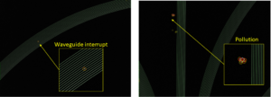
Nobleo is responsible for image processing algorithms to enable a fully automated a camera-based PIC inspection. The image processing algorithms developed in this project are a combination of traditional methods and machine learning algorithms .
In addition to the cosmetic inspection of the wafer, Nobleo is involved in the image based alignment of the wafer within the machine. The alignment shall be done at the borders of what is technically still feasible with an image based camera system.
Once the first prototype is released, a second iteration is planned in which the execution time of the algorithms is improved by parallization of image processing tasks and/or implementation of algorithms in dedicated hardware (FPGA). Implementation in custom hardware shall be done in close co-operation with Technolution.
![]()
![]()